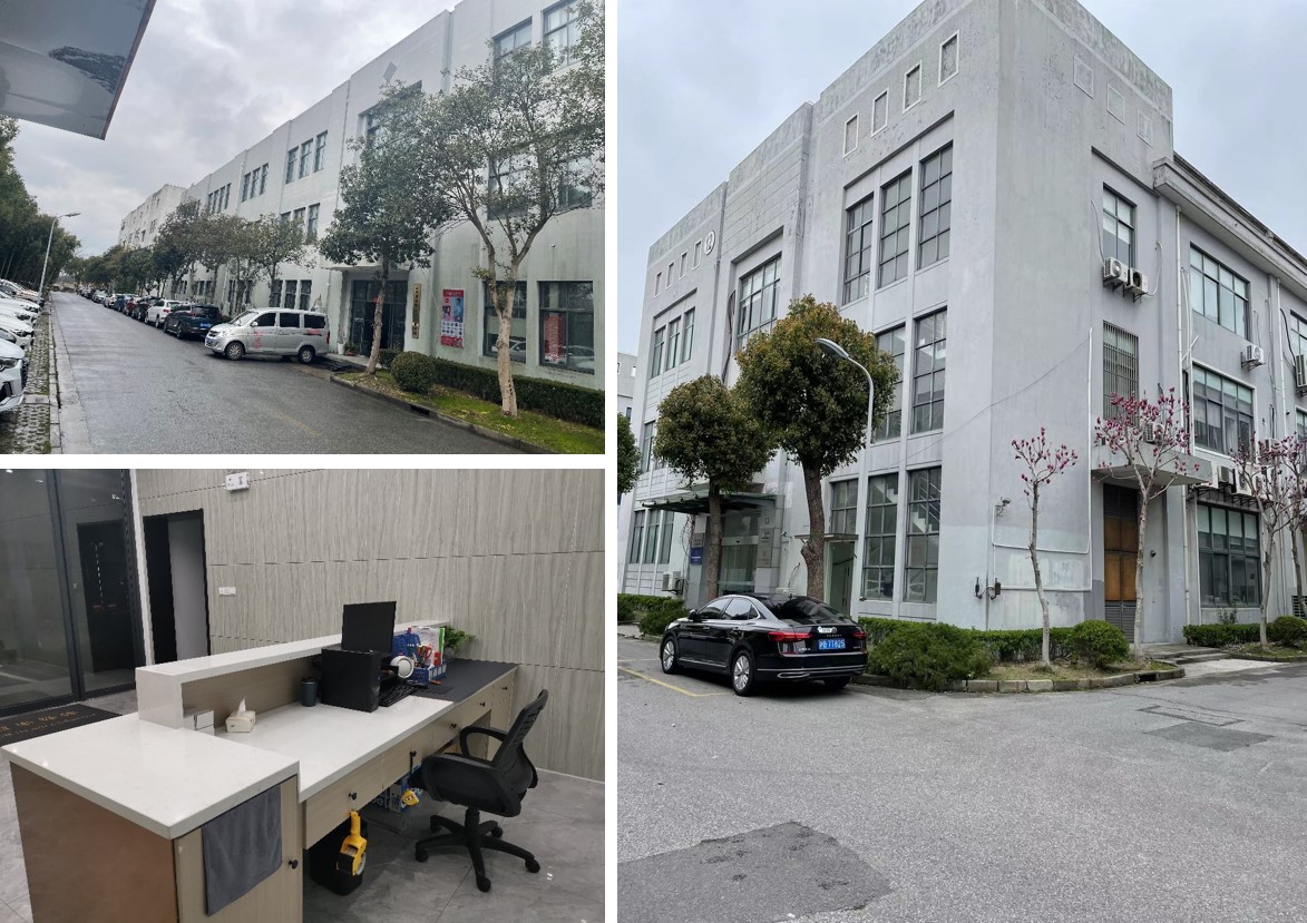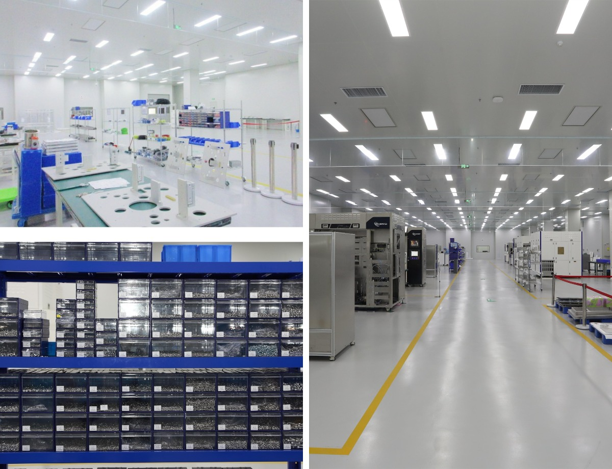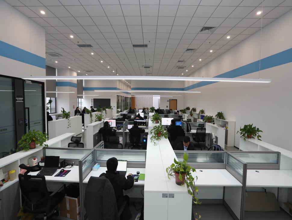
运营服务中心

生产制造基地

办公区
-
Temporary Bonding/Debonding Technologies for Fan-out Packaging
Fan-out wafer-level packaging (FOWLP) is a cost-effective way to achieve high interconnect density and to manage larger I/O counts within an affordable package...
2025 -
一文介绍什么是扇出型封装晶圆级封装(Fan-out WLP)工艺技术
什么是扇出型封装?扇出型封装技术在封装市场是较为热门的话题。在扇出型技术中,裸片直接在晶圆上封装。由于扇出型技术并不需要中介层(interposer),因此比2.5D/3D封装器件更廉价...
2025 -
Semiconductor Back End Processes: Adopting GEM Judiciously
For many years the semiconductor industry’s wafer fabrication facilities, where semiconductor devices are manufactured on [principally] silicon substrates, have universally embraced and mandated the GEM standard on nearly 100% of the production equipment...
2025 -
Semiconductor Back End Processes: Selective GEM300 Adoption
“Advanced Back End Factory Integration” (ABFI) has already decided to promote the adoption of the GEM standard...
2025 -
Novel Approaches to Wafer Handling
Economics are forcing semiconductor manufacturers away from traditional 3D through silicon via (TSV) packaging integration. The future of advanced packaging continues to evolve towards chiplets and innovative new ways to combine specialized microelectronics components. This allows manufacturers to streamline the production for individual “subassemblies” that can then be configured later into functional products...
2025 -
How to Prevent High Wafer Warpage in Fan-in and Fan-out Wafer Level Packaging
Fan-In Wafer-Level Packaging (FI WLP) and Fan-Out Wafer-Level Packaging (FO WLP) are two approaches that are showing promising cost efficiency and performance benefits as indicated by their market growth...
2025
请输入搜索关键字
确定

